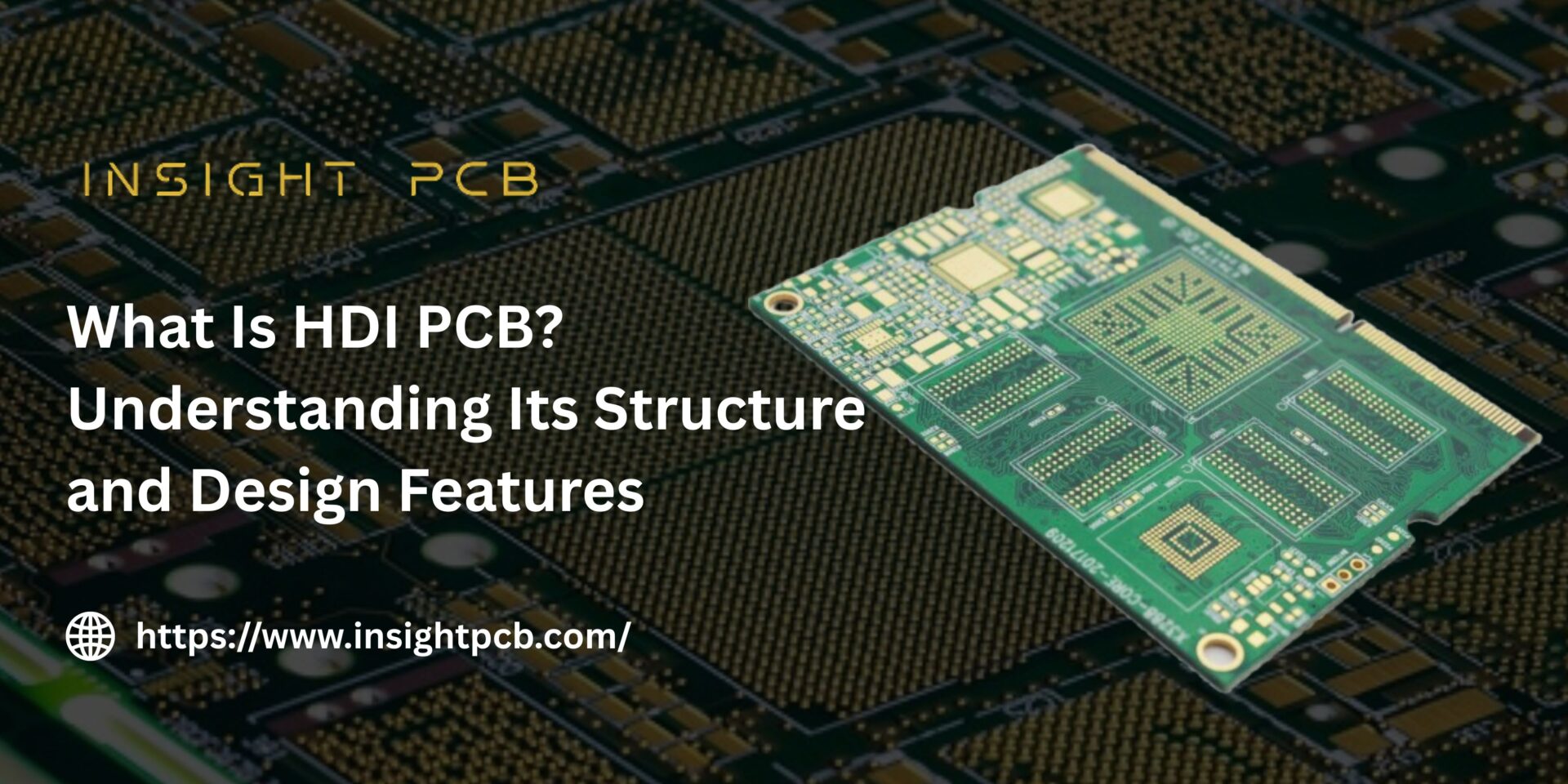
What Is HDI PCB? Understanding Its Structure and Design Features
The demand to fit more functionality into smaller spaces has grown with ongoing technological development. More components are crammed into a smaller area. When researchers began seeking ways to reduce the size of PCB vias, high-density interconnect (HDI) PCB design and production emerged in the 1980s. In 1984, the first sequential printed circuit boards, or industrial build-ups, were introduced. PCBs created with HDI techniques typically have smaller dimensions.
To fit more components into a smaller space, an HDI PCB incorporates blind, buried, and micro vias, as well as vias in pads, and features fragile traces. In this blog, we will discuss what HDI PCB is, its design features, and its applications.
What Is HDI PCB?
The full form of an HDI PCB is High-Density Interconnect. These PCBs allow more circuits and connections to be compressed into less space. They enable thin, compact, and lightweight designs for gadgets, without compromising performance.
Imagine trying to fit a busy city’s traffic network into a tiny town. You’d need smaller streets, more innovative intersections, and careful planning. That’s what HDI PCBs do for electronic signals.
Features That Set HDI PCBs Apart
Not every PCB is similar. HDI PCBs possess a couple of tricks up their sleeve:
- Microvias: Small holes that pass between layers of the board, much smaller than standard vias.
- Blind and Buried Vias: These pass between specific layers without passing entirely through the board, keeping things more compact.
- Thin Traces and Tight Spacing: Electrical traces are thinner and closer together. It enables more parts placement in less space.
- Multiple Layers: Some HDI PCBs have 12 or more layers. It depends on the functionality of the device.
These attributes make HDI PCBs a good choice when space and performance are equally important.
How the Structure of HDI PCBs Works
HDI PCBs aren’t just about stacking circuits; they’re thoughtfully designed. Their construction allows signals to travel efficiently, components to be hand-in-glove, and the board to be reliable.
Layers Explained
Most HDI PCBs contain three primary types of layers:
- Substrate Layer: The foundation supporting the entire board. Typically composed of materials such as FR4 or other composites.
- Internal Layers: Support signals and power across the board. Joined with microvias or buried vias.
- Surface Layers: Where the components are soldered in place. Generally, use blind vias to connect to inner layers without occupying additional space.
This layering is what makes HDI PCBs so compact and efficient.
The Role of Microvias
Microvias are small but mighty. They make high-density circuit layouts feasible. Some key things about them:
- Laser-drilled for accuracy
- They typically connect one or two layers at a time.
- Minimize signal interference
- Can be stacked for even tighter connections
Without microvias, it would be almost impossible to pack so many circuits onto a tiny board.
Why Select HDI PCBs?
HDI PCBs are best for several vital reasons. These offer advantages that a conventional PCB cannot:
- Smaller Devices: Perfect for slim smartphones, wearables, and ultrathin laptops.
- Electrical Performance: Shorter traces make faster, more reliable signals.
- More Components in Smaller Board Area: Ideal for meeting the demands of today’s electronics from a compact board.
- Reliability: Better chances of avoiding soldering defects due to precise and tiny vias.
- High-Frequency Capability: Consider 5G and high-end computing applications.
These benefits are the reasons HDI PCBs are becoming the norm for high-tech devices.
Where HDI PCBs Are Implemented
HDI PCBs are found in equipment we all use daily. Here’s a quick rundown:
- Smartphones and tablets
- Laptops and ultrabooks
- Wearable technology such as smartwatches and fitness trackers
- Medical devices for diagnosis and monitoring.
- Test equipment featuring 5G modules
If a device is small yet high-performing, it may be using an HDI PCB design.
HDI PCB Design: The Essentials
Making a design for an HDI PCB differs from that of an ordinary board. These are a few points to be taken into consideration.
- Material selection, thickness of the substrate, and copper will affect its performance.
- Proper planning of blind, buried, or stacked vias affects reliability and density.
- More layers mean more interconnects, but also more complexity.
- High-speed signals must be routed carefully so as not to interfere.
- Fine etching and laser drilling ensure a consistent finish.
A well-made HDI PCB will work better and last longer, especially in small, demanding devices.
Difficulties with HDI PCBs
HDI PCBs are powerful, but they come with trade-offs:
- Higher Cost: Advanced design and manufacturing techniques cost more.
- Complex Assembly: Finer vias and traces require accurate soldering.
- More Difficult to Fix: Tightly packed configurations may be difficult to diagnose.
- Design Restrictions: Not all circuits are suitable for a close HDI design.
Nevertheless, for those devices where space and performance are important factors, the advantages tend to outweigh the drawbacks.
Conclusion
HDI PCBs are revolutionizing electronics design. With microvias, layers, and tight routing, they enable tiny devices to be faster, more robust, and better equipped to deal with current requirements. Knowing what HDI PCB is helps value why devices today are getting smaller and have more features than the ones before.
So the next time your smartphone, smartwatch, or medical device works smoothly, an HDI PCB is likely doing the hard work behind the scenes.
For professional-grade HDI PCB solutions, InsightPCB offers precision, reliability, and expertise. We are trusted by leading technology companies worldwide. Contact us today to learn more.