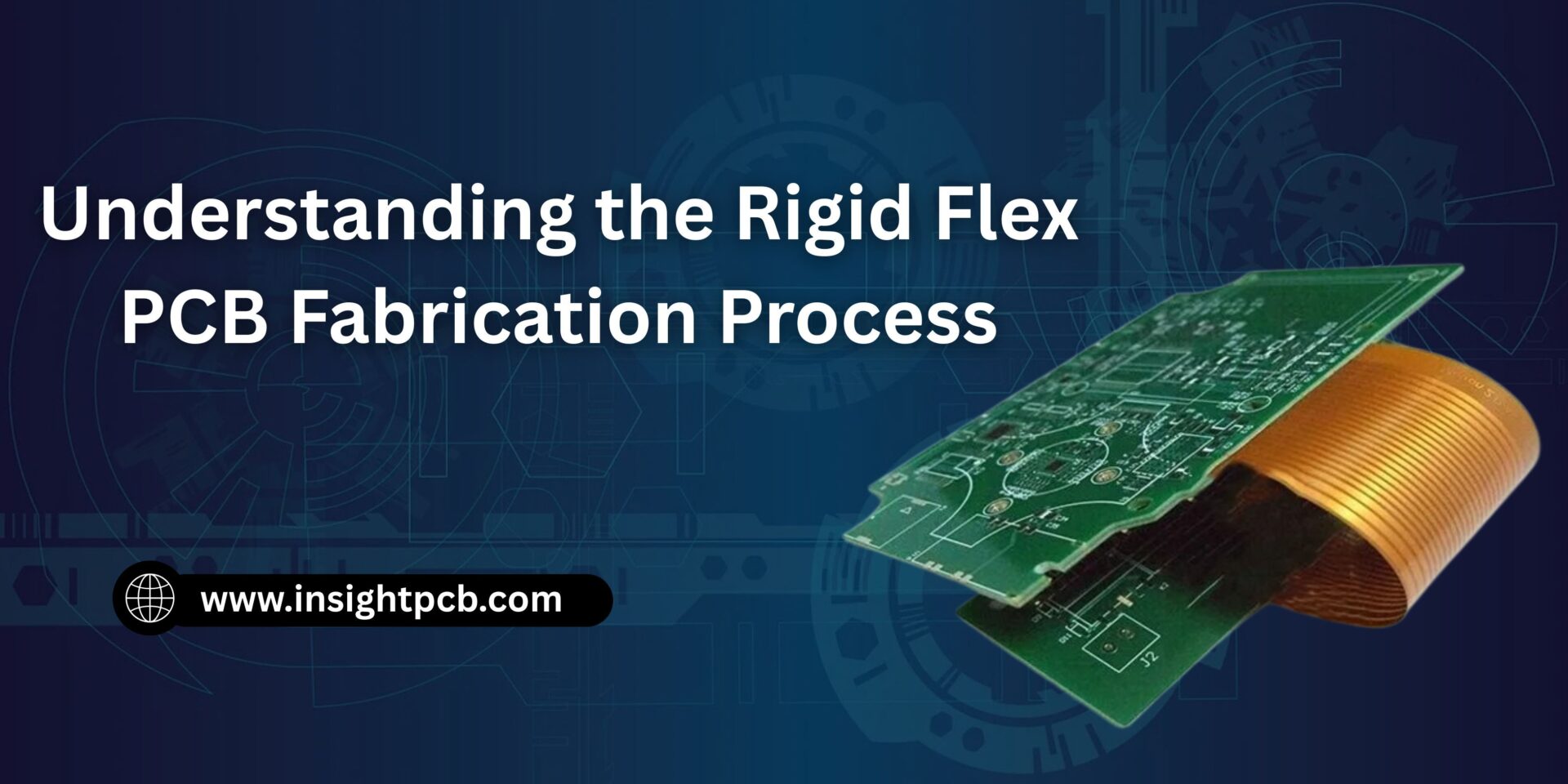
Understanding the Rigid Flex PCB Fabrication Process
The parameters of design are becoming increasingly intricate, and typical PCB solutions often cannot accommodate these designs. That is where rigid flex PCB fabrication comes in to the rescue. With the reliability of rigid boards and the flexibility of flex circuits, rigid-flex PCBs are the driving force behind the majority of today’s high-technology products, ranging from medical devices and space products to contemporary consumer electronics.
In this blog, we will guide you through the entire rigid flex PCB manufacturing process, breaking down each step to make it easier to understand how these extremely efficient boards are created.
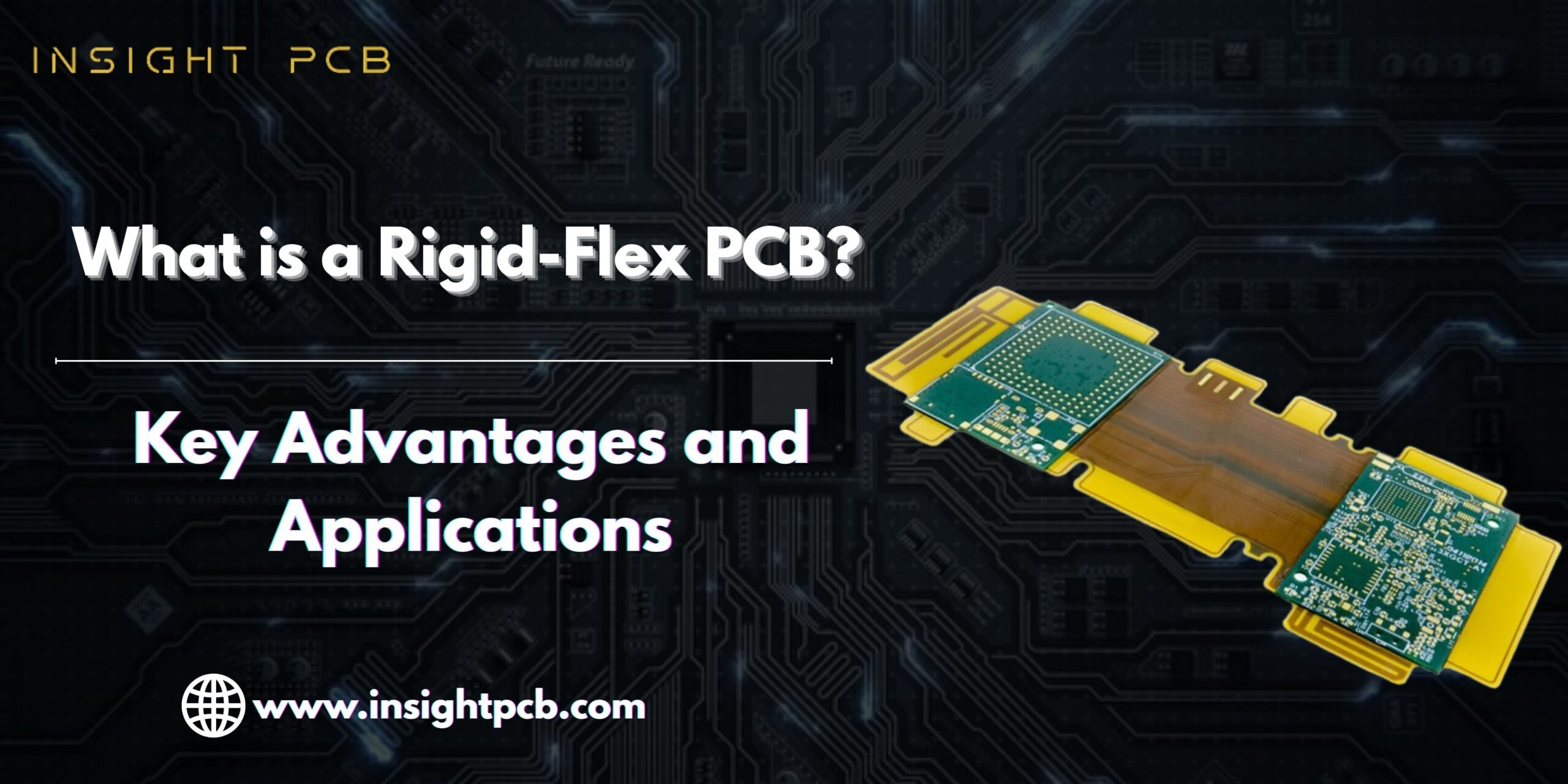
What is a Rigid Flex PCB?
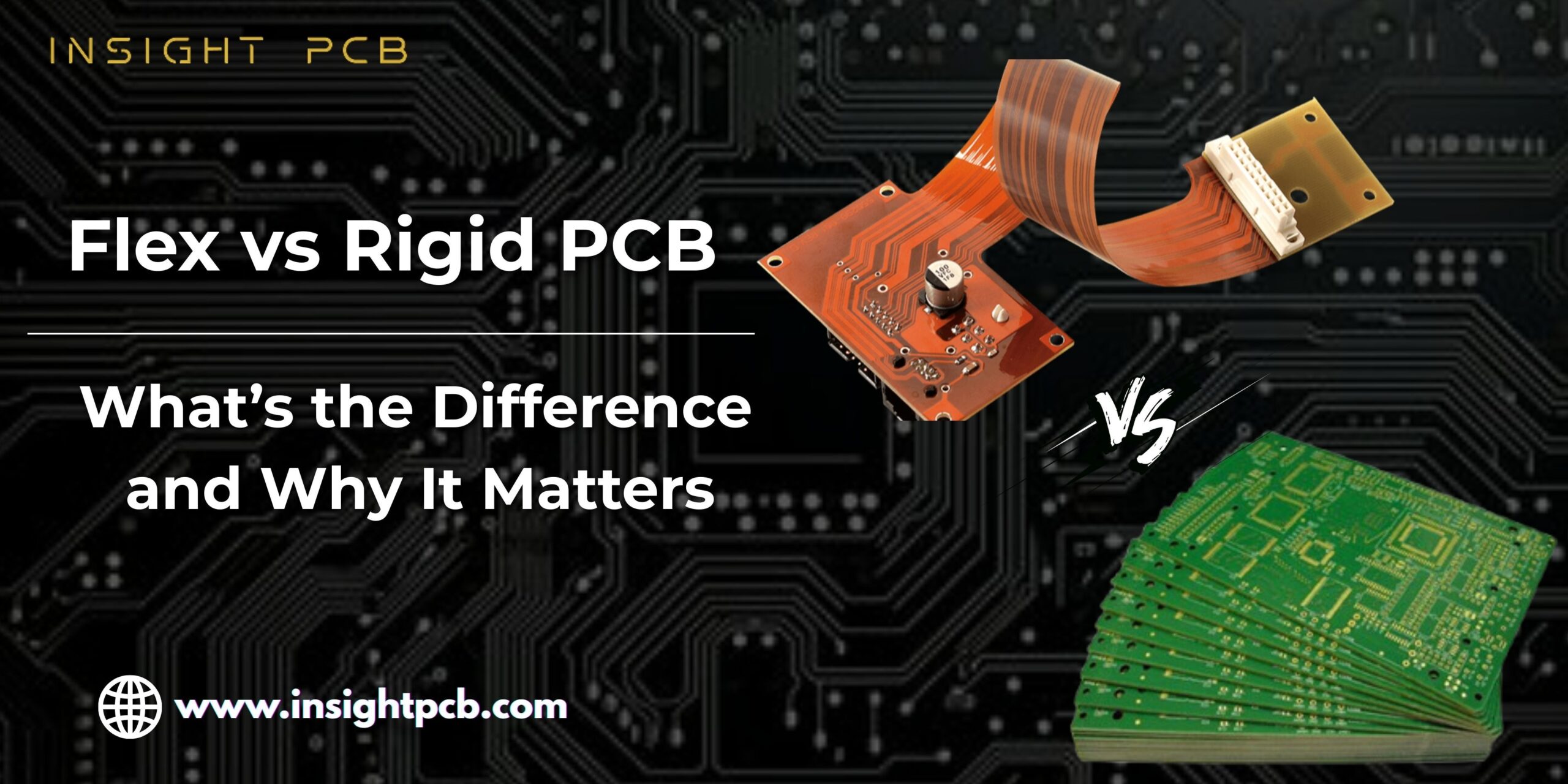
A rigid-flex PCB is a hybrid panel that combines rigid and flexible substrates in a single structure. While conventional PCBs are rigid or flexible, rigid-flex PCBs enable developers to create robust, thin, and lightweight circuits. The form in such a state minimizes connectors, improves signal integrity, and makes boards more reliable for high-demand applications.
Technically, it is rigid enough to hold components in place and flexible enough to be placed in tight areas during rigid flex PCB production.
Step-by-Step Process for Producing Rigid Flex PCB
Producing a rigid-flex PCB is a process that requires advanced technology and precision. The following is the overview of steps involved in the process:
1. Design and Material Selection
It starts with material selection and circuit design. The designers determine where stiffness is required and where flexibility is needed in the circuit. Polyimide is typically used in flexible areas due to its thermal resistance and flexibility, while FR4 material is generally used in stiff areas.
2. Imaging and Etching
After the design is finalized, copper layers are laminated onto the desired substrate. The circuit designs are printed onto the board using photolithography. Excess copper pieces are removed using etching. It leaves only the right traces to deliver connectivity.
This is a crucial step in rigid flex PCB fabrication, as accuracy allows the board to adjust the complex interconnects found in modern electronics.
3. Rigid and Flex Layer Lamination
The true magic of rigid-flex PCBs lies in combining rigid and flexible components. Flexible circuits are laminated into a multi-layer structure, and rigid layers are employed in the areas that require them. Warmth and force are used to bond the material without destroying the flexible parts.
The multi-layer lamination delivers a seamless collaboration of rigid and flexible elements. It translates into improved stability and performance.
4. Via Formation and Drilling
During lamination, accurate holes, referred to as vias, are drilled to provide interconnection between layers. Depending on the design, mechanical drilling or laser drilling is performed. Vias are copper-plated for conductivity following drilling.
5. Copper Deposition and Plating
Subsequently, the drilled vias are plated, creating conductive paths through the deposition of copper. This process secures reliable electrical connections between all the layers of the board. Additionally, uniform plating is also necessary to achieve high reliability, especially in applications that are vibrated or mechanically stressed.
6. Solder Mask and Surface Finish
A solder mask is screen-printed over the copper traces to save them from oxidation and solder bridges during assembly. Exterior finishes, such as ENIG (Electroless Nickel Immersion Gold), HASL (Hot Air Solder Leveling), or OSP (Organic Solderability Preservative), are deposited onto the places before fusing.
7. Profiling and Cutting
Once the fabrication method is nearly done, the panel is profiled or cut to its final shape using punching, routing, or laser cutting. This is a crucial stage to confirm the PCB fits correctly inside the targeted device housing spot.
8. Testing and Quality Control
Rigid-flex PCBs experience ample testing before shipping to provide functionality and dependability. They are stress, electrically, and continuity-tested to ensure that any faults or defects are identified.
In medical and aerospace applications, strict and rigid quality specifications are required; thus, this process is the backbone of the rigid-flex PCB manufacturing process.
Main Benefits of Rigid Flex PCBs
Knowledge of manufacturing is why stiff-flex PCBs are a top priority in most industries. The main benefits are:
- Space Efficiency: The small size allows circuits to be housed in close cases without compromising performance.
- Better Dependability: Fewer connectors and solder ends stop failure points.
- Reliability: Resistant to shock, vibration, and flexing.
- Configuration Flexibility: Supports 3D product design layouts.
- Better Performance: Superior signal integrity than conventional connectors.
Issues with Rigid Flex PCB Production
Where beneficial, production is not free of issues:
- Difficult Production: Rigid and flexible substrates require specialized skills and advanced machinery for assembly and integration.
- Increased Cost: They are more costly than regular PCBs due to the process and materials built into them.
- Design Difficulty: Requires careful design to avoid stressing areas in the flex area.
Working with Insight PCB assures that these problems are addressed, and you obtain high-quality boards that fulfill your needs.
Conclusion
The future is electronic and is based on creation in PCB design and production. Rigid-flex PCBs deliver the best performance, flexibility, and durability. When organizations experience the fabrication method, they learn the importance of using panels with this technology.
If you require reliable and accurate rigid flex PCB fabrication, you will need to find an experienced manufacturer. At Insight PCB, we ensure that you get the best rigid flex PCB product well beyond the highest industrial standards. With our expertise, your projects are equipped with the newest technology and guaranteed reliability.