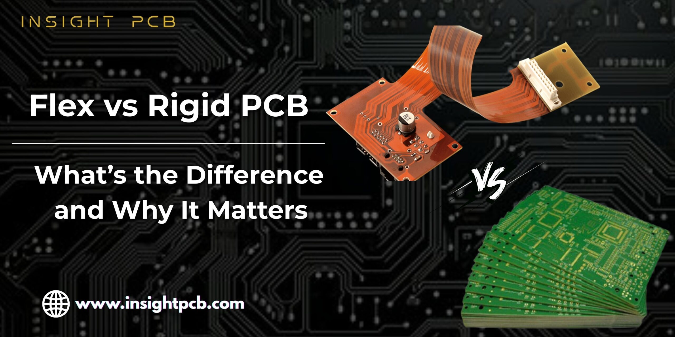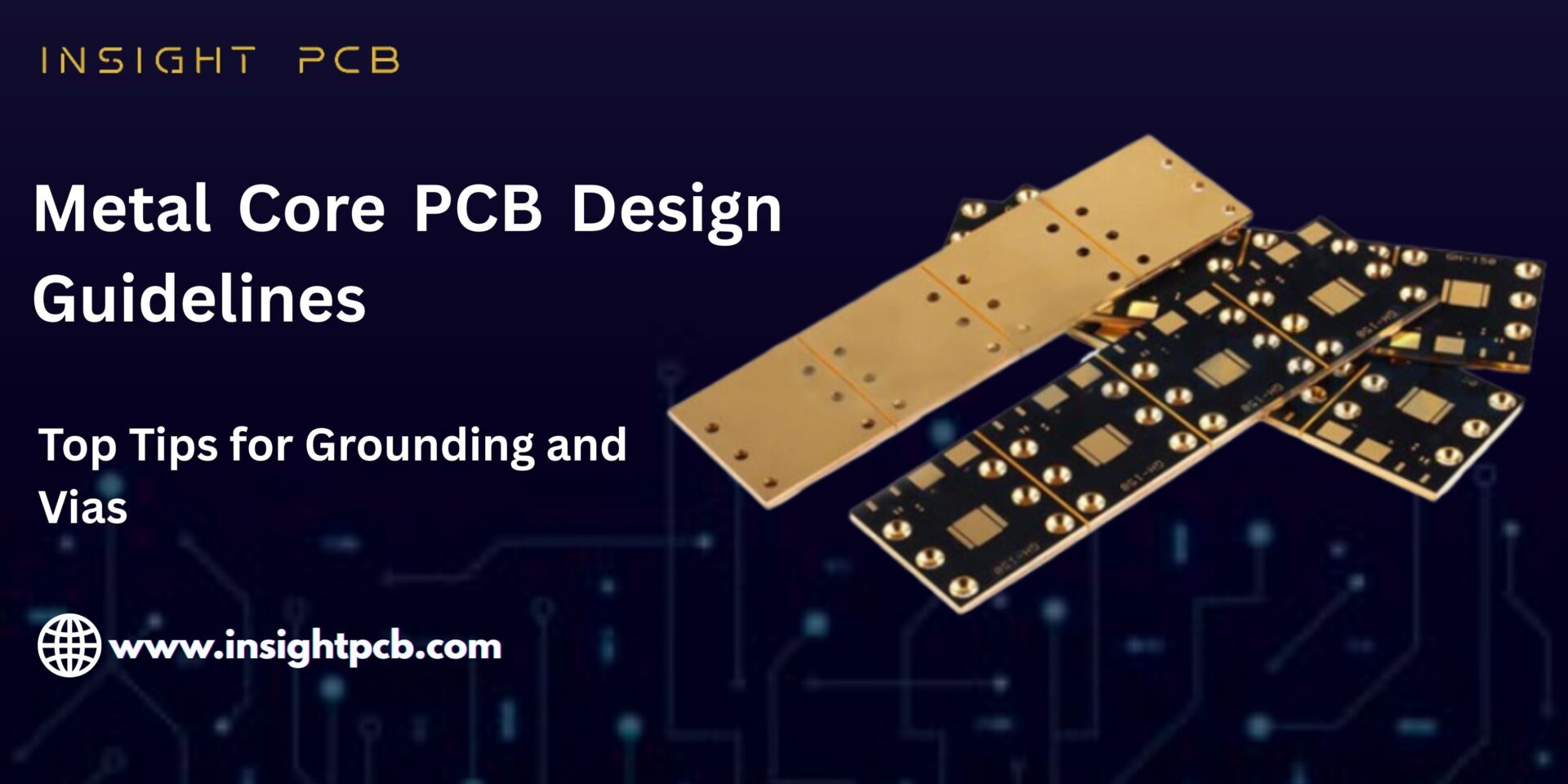
Metal Core PCB Design Guidelines: Top Tips for Grounding and Vias
Designing with metal core PCBs requires special attention. The boards incorporate a metal, commonly aluminum or copper, under the circuitry to dissipate high heat and mechanical stress. In this blog, you’ll learn the best metal core PCB design guidelines, with a focus on grounding and via placement. When done right, these practices enable you to design robust, high-performance boards. Whether your metal core PCB is used with LED applications, power conversion, or industrial control, these ideas will improve your design.
Understanding Metal Core PCB Benefits
Metal core PCBs shine in high-heat situations. Compared to standard FR4:
- Heat is pulled through the metal layer, reducing hot spots that damage traces or components.
- The metal provides mechanical strength and resists warping.
- It minimizes electromagnetic interference by being a grounded plane.
These characteristics render such PCBs ideal for high-power circuits, while FR4 boards can overheat.
Grounding Guidelines on Metal Core PCBs
Grounding is essential to ensure signal integrity, control EMI, and safety. Here are proven practices:
- Use the Metal Core as a Ground Plane
Tie the metal substrate to ground for shielding or to dissipate power excess. If used as a heat spreader, leave its underside ungrounded to avoid ground loops.
- Clearance Around Component Vias
Double-sided boards require plated vias. Use an antipad around metal-contacting vias to insulate signals from the metal layer.
- Dedicated Ground Layer
In multi-layer designs, reserve an entire internal layer for ground. It offers a clean return path and helps with EMC.
- Minimize Ground Loops
Route analog and digital grounds separately, merging them at a single point. It avoids interference paths.
- Avoid Interrupting Ground Planes
Keep ground layers intact, no splits or slots. Breaks increase impedance and EMI susceptibility.
- Via Stitching Near Edges
Place stitching vias to tie signal layers to the metal core or ground plane. It strengthens EMI shielding and maintains uniform ground potential.
Best Via Practices for Heat and Signal Management
Vias in metal-core PCBs need extra care to balance signal routing and thermal conduction:
- Thermal Vias
A grid of small vias near heat-generating parts conducts heat to the metal core or secondary planes.
- Blind and Buried Vias
In double-sided boards, use insulated blind/buried vias to connect signal layers to the metal core without risking shorts.
- Stacked Via Layout
For high-density signals, stack microvias, blind vias, and through-vias carefully. Use CAD tools to manage limits, as in HDI design.
- Avoid Via Overcrowding
Too many vias increase distortion in metal planes. Use them only where needed for grounding or valid routing.
- Thermal Relief Pads
Use spoke-like thermal reliefs on large copper pads to maintain solderability by controlling heat transfer while assembling.
Stack-Up and Layering for Best Results
Metal core PCBs often follow a specific stack-up:
- Metal backplane – unplated, used for heat dissipation.
- Thermal dielectric layer – insulated, transferring heat.
- Circuit layers – single or double-sided layout.
For double-sided, ensure drilled, insulated vias and proper paddings are in place. Avoid routing on the metal backplane except in grounded zones.
Choosing Materials and Thermal Dielectrics
Aluminum is inexpensive and thermally conductive. Copper offers higher performance when the budget allows. Dielectric layers need low thermal resistance and high breakdown voltage. Consult your board house to select the right material and thickness for your application.
Validation and Testing Tips
Good design validation prevents costly rework:
- Ground impedance tests – ensure low impedance return paths.
- Thermal simulation – spot thermal hotspots early.
- EMI testing – verify ground plane function and shielding.
- Power cycling – test board under thermal stress for reliability.
These validation steps are essential to confirm your layout meets performance goals.
Common Mistakes to Avoid in Metal Core PCB Design
Even experienced designers can fall into traps when working with metal core PCBs. Avoid these pitfalls to save time and cost:
- Forgetting Isolation Gaps
Insulate the metal core correctly from signal vias. Overlooking clearance rules can cause electrical arcing under high voltage.
- Overusing Thermal Vias
While they aid in heat dissipation, excessive thermal vias can weaken mechanical integrity or interfere with routing.
- Improper Core Grounding
Randomly tying the metal core to multiple grounds creates loops and EMI issues. Always follow a controlled grounding scheme.
- Ignoring Thermal Expansion Differences
Metal cores expand differently from FR4 or components. Failing to account for this can cause solder joint cracking over thermal cycles.
- Choosing the Wrong Dielectric Thickness
A thickness that’s too thin will result in breakdown voltage problems. If it’s too thick, thermal conductivity is compromised.
By avoiding these errors, you enhance yield, reliability, and performance.
Why Insight PCB Works with Metal Core PCB Designs
At Insight PCB, our team has thermal and signal ground expertise in each project. We:
- Design stack-ups that balance thermal efficiency with signal integrity.
- Use vias strategically for both heat and ground pathways.
- Employ CAD tools to prevent EMI issues before fabrication.
Our approach follows the leading metal core PCB design guidelines. So, your product works correctly under high heat and signal conditions.
Pro Tips for Next-Level Designs
- Use CAD constraint managers, such as in OrCAD X, to control via types, sizes, and clearances.
- Build ground plane islands for isolated analog zones.
- Create fences for RF paths to reduce electromagnetic coupling.
- Check your layout with DFM and EMI tools early in the design phase.
Conclusion
Metal core PCB design requires careful stacking, grounding, and thermal routing. Grounding the metal core, separating vias, and stitching ground planes help to maintain low EMI and clean signal paths. Thermal vias draw heat away from critical components, and simulation confirms the design performance. Adherence to these metal core PCB design guidelines guarantees longevity for products subjected to heat, switching loads, or high-frequency signals.
Rely on Insight PCB to implement these best practices. Our process ensures your boards are thermally efficient, electrically sound, and ready for real-world use.